TL;DR
Tearing down an eCos-based embedded system from flash dump to boot sequence.
Flash Dump
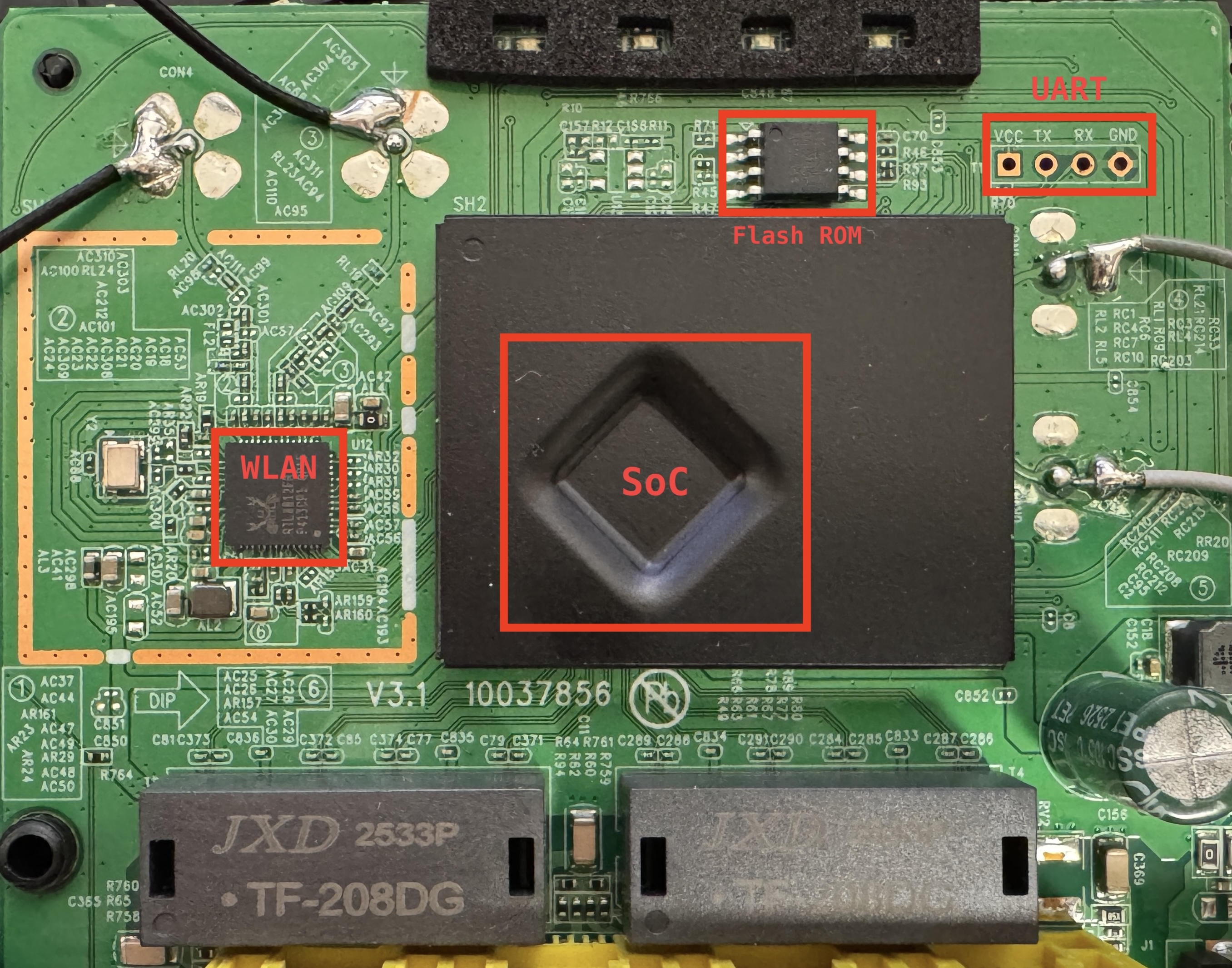
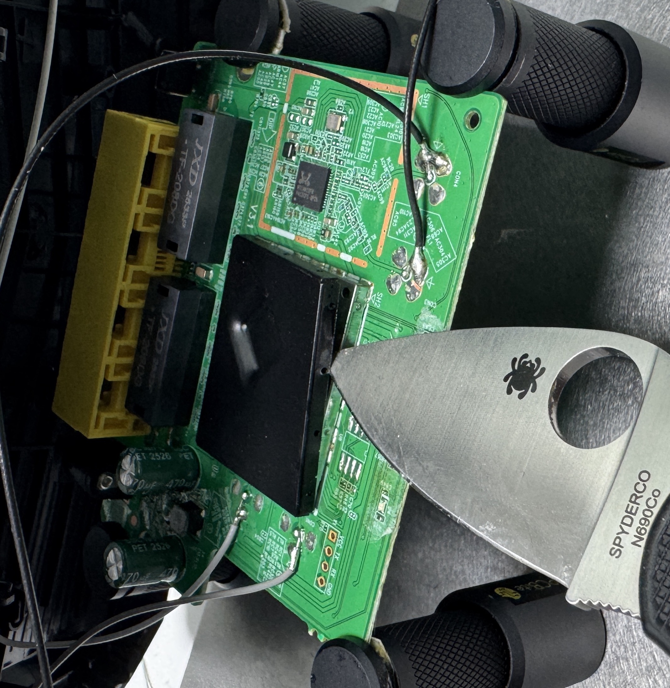
The eCos-based router target had a SoC (System-on-Chip), SPI SOP-8 NOR flash chip, UART (Universal Asynchronous Receiver-Transmitter) interface and Wireless LAN chip. For dumping the flash memory I just decided to chip off the NOR flash.


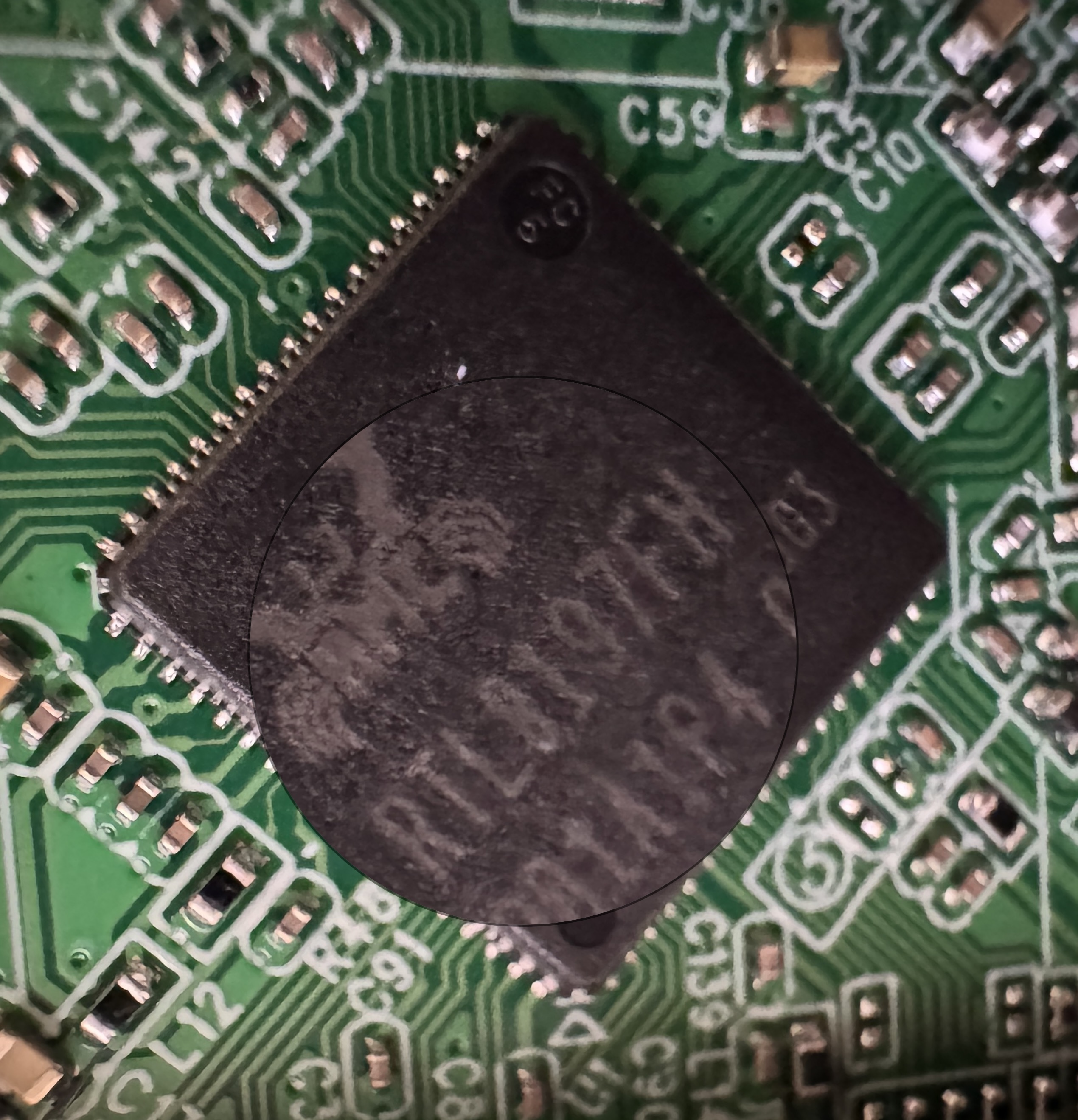
The NOR flash was a BoHong BH25D16A chip and the pin map was as shown below:
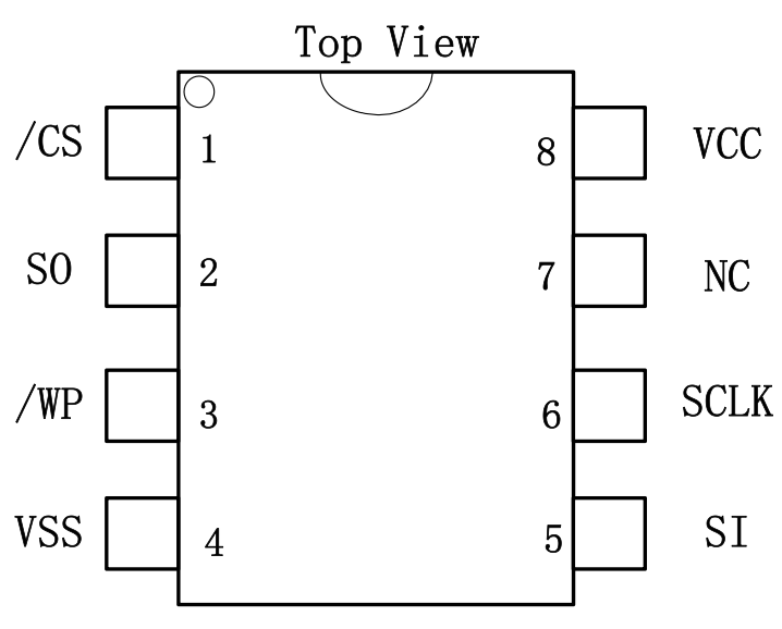
- 1: /CS (Chip Select)
- 2: DO (Serial Data Output)
- 3: /WP (Write protect when driven LOW)
- 4: VSS (Ground)
- 5: DI (Serial Data Input)
- 6: SCK (Serial Clock)
- 7: NC (Not Connection)
- 8: VCC (Supply Voltage)
The BH25D16A was designed for environments where it has dedicated (non-shared) access to the SPI bus, so there is no /HOLD pin for sharing the bus to other devices. And because I only read the flash memory, I left the /WP pin floating (not needed for read-only operations).
SPI
┌──────────┐                     ┌──────────┐
│          │──── MOSI (SDI) ────>│          │
│          │<─── MISO (SDO) ─────│          │
│  Master  │──── SCLK (CLK) ────>│  Slave   │
│          │──── CS/SS (LOW) ───>│          │
└──────────┘                     └──────────┘
SPI (Serial Peripheral Interface) is a synchronous serial communication protocol in which one master communicates with one or more slave devices in full-duplex. In case of memory dump, the master is the SPI programmer and the slave is the memory chip.
| Pin | Direction | Description |
|---|---|---|
| MOSI(Master Out Slave In) | Master → Slave | Master’s data send line |
| MISO(Master In Slave Out) | Slave → Master | Slave’s data send line |
| SCLK(Serial Clock) | Master → Slave | Master’s clock signal |
| CS/SS(Chip Select / Slave Select) | Master → Slave | Selects slave with driven LOW |
Clock Signal
SCLK  __/‾\_/‾\_/‾\_/‾\__
MOSI  -[1]-[0]-[1]-[1]---
        ↑   ↑   ↑   ↑
      Send 1 bit per clock edge
The clock signal acts like a timing signal that tells devices when to read or write data, ensuring that multiple devices remain synchronized during communication. The master defines the clock, and the slave samples data on the clock edge (the rising edge of SPI mode 0/3).
SPI Communication Diagram
CS   ‾‾‾‾\___________________________________/‾‾‾‾
        ↑ CS LOW (communication start)       ↑ CS HIGH (communication stop)

SCLK _______/‾\_/‾\_/‾\_/‾\_/‾\_/‾\_/‾\_/‾\_______
            1   2   3   4   5   6   7   8
            ↑ Send 1 bit per clock edge

MOSI ────[MSB]──────────────────────────[LSB]─────  (Master → Slave)
MISO ────[MSB]──────────────────────────[LSB]─────  (Slave → Master)
         ↑ Full-Duplex
The BH25D16A’s maximum clock frequency is 55 MHz for normal read and 108 MHz for fast/dual read. I used a CH341A programmer to communicate with the NOR flash via SPI. Because the flashrom‘s spispeed was fixed at 2 MHz, which is within the maximum clock frequency range of the NOR flash, I was able to read the flash memory without speed adjustment.

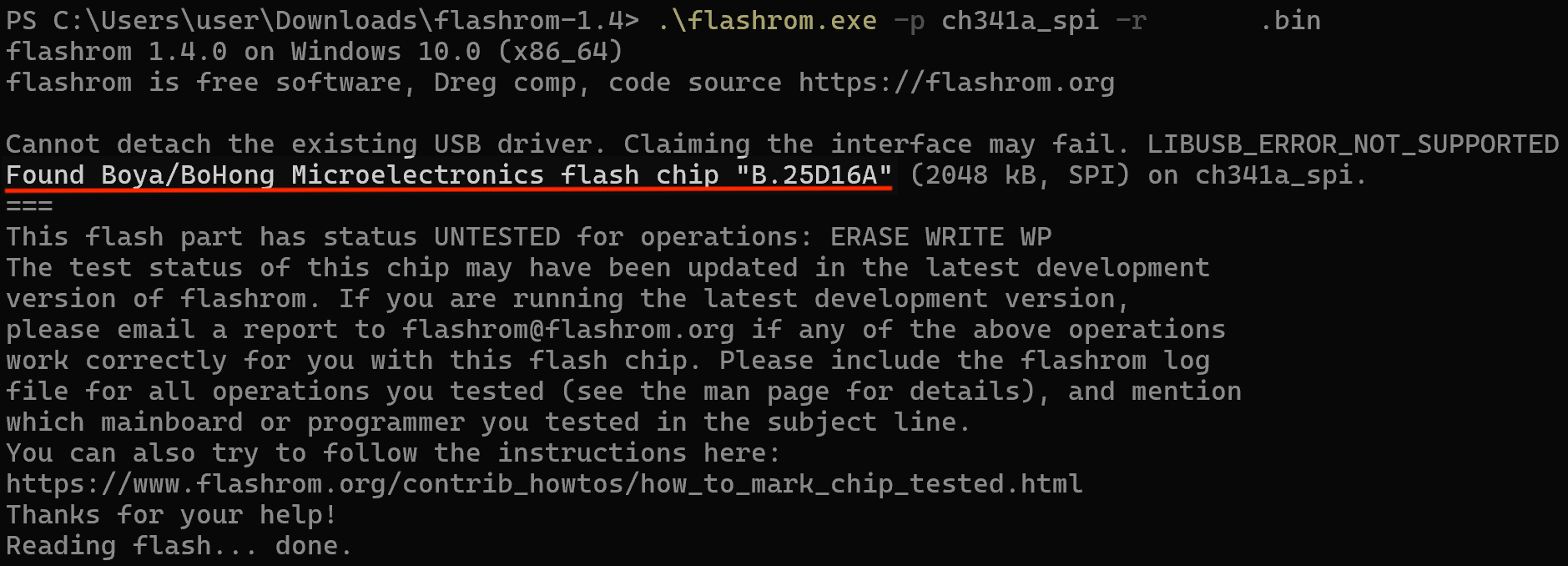
To verify the stability of the firmware that I read, I extracted it twice and compared the MD5 hash of each binary.

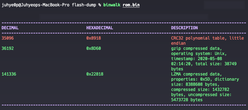
The binary MD5 hash was identical. The firmware contains gzip compressed data and LZMA compressed resources. The LZMA compressed resources will be decompressed to RAM at the boot sequence. Before performing static analysis, I needed to identify the SoC’s memory map in order to create a segment mapped to the correct memory address.
Thus, I removed the EMI (Electromagnetic Interference) shield to check the SoC model. It belongs to the RTL8197F family, which is based on the MIPS architecture.
Boot Sequence Overview

Boot Stage 1

According to the RTL8197F datasheet, the Stage 1 Boot ROM code executes at virtual address 0xB0000000 using XIP (eXecute In Place) technology.
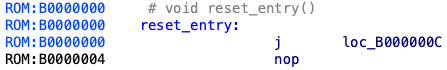
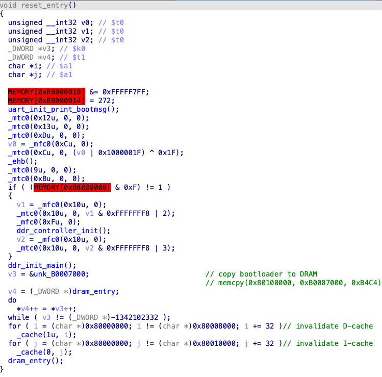
The Stage 1 Boot ROM code prints boot logs, invalidates the D-cache (Data cache) and I-cache (Instruction cache), loads the Stage 1.5 Bootloader (0xB0007000) to DRAM (0x80100000), and jumps to it.
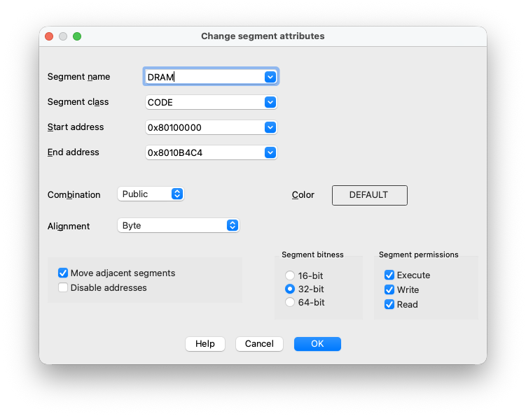
So I created a new DRAM segment like below:
Boot Stage 1.5
DRAM:80100000     # int dram_entry()
DRAM:80100000    dram_entry:
DRAM:80100000                    li      $t0, unk_8010B4C0
DRAM:80100008                    nop
DRAM:8010000C                    addi    $t0, 0x2000
DRAM:80100010                    nop
DRAM:80100014                    move    $sp, $t0
DRAM:80100018                    nop
DRAM:8010001C                    jal     boot_stage1_5_main
DRAM:80100020                    nop
DRAM:80100024                    nop
DRAM:80100028                    nop
DRAM:8010002C                    nop
DRAM:8010002C     # End of function dram_entry
...

int boot_stage1_5_main()
{
  int v0; // $a0
  int v1; // $a1
  int v2; // $a2
  int v3; // $a3
  unsigned int v5; // [sp+20h] [-Ch] BYREF
  int v6; // [sp+24h] [-8h] BYREF

  v5 = 0x7FFFFFFF;
  v6 = 0x7FFFFFFF;
  gzip_decompress(byte_80101D60, &v5, 0x80000000, &v6); // gzip_decompress(0x80101D60, &in_size, 0x80000000, &out_size)
  post_decompress_init();                       // D-cache writeback + I-cache invalidate — synchronize released code cache
  return MEMORY[0x80000000](v0, v1, v2, v3);    // jalr 0x80000000 -> Stage 2 Bootloader("RTL8197F-VG boot version:614")
}
The Stage 1.5 Bootloader decompresses the gzip compressed Stage 2 Bootloader (0x80101D60) to KSEG0 (0x80000000), synchronizes the instruction and data caches (D-cache writeback + I-cache invalidate), and executes it.
Boot Stage 2
DRAM:80000000     # Segment type: Pure code
DRAM:80000000                    .text # DRAM     // vector table
DRAM:80000000                    b       loc_8000040C     # DATA XREF: sub_80003130+70↓o
DRAM:80000004                    nop
DRAM:80000004     # ---------------------------------------------------------------------------
DRAM:80000008                    .byte    0
...

DRAM:8000040C     # ---------------------------------------------------------------------------
DRAM:8000040C
DRAM:8000040C    loc_8000040C:                            # CODE XREF: DRAM:80000000↑j
DRAM:8000040C                    mtc0    $zero, WatchLo   # Memory reference trap address low bits
DRAM:80000410                    mtc0    $zero, WatchHi   # Memory reference trap address high bits
DRAM:80000414                    mtc0    $zero, Cause     # Cause of last exception
DRAM:80000418                    mfc0    $t0, SR          # Status register
DRAM:8000041C                    li      $at, 0x1000001F
DRAM:80000424                    or      $t0, $at
DRAM:80000428                    xori    $t0, 0x1F
DRAM:8000042C                    mtc0    $t0, SR          # Status register
DRAM:80000430                    ehb
DRAM:80000434                    mtc0    $zero, Count     # Timer Count
DRAM:80000438                    mtc0    $zero, Compare   # Timer Compare
DRAM:8000043C                    lui     $sp, 0x8070
DRAM:80000440                    nop
DRAM:80000444                    li      $s0, 0x80018B90
DRAM:8000044C                    li      $s1, 0x80437F10
DRAM:80000454                    move    $t0, $s0
DRAM:80000458
DRAM:80000458    loc_80000458:                            # CODE XREF: DRAM:80000460↓j
DRAM:80000458                    sw      $zero, 0($t0)
DRAM:8000045C                    addi    $t0, 4
DRAM:80000460                    bne     $t0, $s1, loc_80000458
DRAM:80000464                    nop
DRAM:80000468                    nop
DRAM:8000046C                    jal     sub_8000B7E0    // main initialization
DRAM:80000470                    nop
DRAM:80000474                    nop
DRAM:80000478
DRAM:80000478    loc_80000478:                            # CODE XREF: DRAM:loc_80000478↓j
DRAM:80000478                    b       loc_80000478
DRAM:8000047C                    nop
...
int sub_8000B7E0()
{
sub_8000B7A8();
return ((int (*)(void))((unsigned int)sub_8000C328 & 0xDFFFFFFF))();
}
int sub_8000C328()
{
unsigned __int32 v0; // $at
_BYTE v2[16]; // [sp+20h] [-10h] BYREF
MEMORY[0x800247F0] = 0;
MEMORY[0x800247F4] = 0;
init_rt_uart_1();
sub_8000E294();
sub_80000CA4();
sub_8000E270();
sub_8000C1B8();
set_gpio_register(19, 1); // maybe set uart baudrate to 38400
if ( check_PABCD_DAT_register() )
{
sub_8000D5E0();
recovery_mode();
}
print_boot_info(0);
v0 = _mfc0(0xCu, 0);
_mtc0(0xCu, 0, v0 | 1); // enable interrupt
// mtc0 SR |= 1
_ehb();
sub_80000DF4();
sub_8000D5E0();
sub_8000CFFC(4);
sub_8000D5E0(
"port link 0x%x 0x%x 0x%x 0x%x\n",
MEMORY[0xBB80412C],
MEMORY[0xBB804130],
MEMORY[0xBB804134],
MEMORY[0xBB804138]);
sub_8000D5E0("irq:0x%x\n", MEMORY[0xB8003000]);
sub_80002E3C();
sub_80002E3C();
MEMORY[0xB8003000] &= ~0x8000u;
MEMORY[0x80018BC4] = 0;
return firmware_load(1, 0, (int)v2);
}
int __fastcall firmware_load(int a1, int a2, int a3)
{
_BYTE v5[8]; // [sp+18h] [-8h] BYREF
if ( !a1 )
sub_8000E22C();
if ( sub_8000E4C0(1200000000) == 1 )
{
sub_8000D3D4("\nEscape booting by user\n");
sub_8000E22C();
}
if ( !check_firmware_integrity(a3, v5) )
sub_8000E22C();
return load_firmware_n_jump(MEMORY[0x80018BC4], a3);
}Stage 2 Bootloader: Firmware Integrity Verification
int __fastcall check_firmware_integrity(int a1, int a2)
{
  int result; // $v0
  _BYTE v3[8]; // [sp+18h] [-14h] BYREF
  unsigned int v4; // [sp+20h] [-Ch]
  unsigned int v5; // [sp+24h] [-8h]

  MEMORY[0x80018BC4] = 0xB0020000;
  result = check_firmware_header(0xB0020000, a1, a2);
  if ( result == 2 )
  {
    sub_80008F40(v3, 0x20000, 16);
    return verify_rootfs_checksum(
             (HIBYTE(v5) | (v5 << 24) | ((v5 & 0xFF00) << 8) | ((v5 & 0xFF0000) >> 8))
           + (HIBYTE(v4) | (v4 << 24) | ((v4 & 0xFF00) << 8) | ((v4 & 0xFF0000) >> 8))
           - 1342177264);
  }
  return result;
}

int __fastcall check_firmware_header(int a1, _DWORD *a2)
{
  ...
  if ( !sub_80008F40(a2, a1, 16) )
  {
    sub_8000D3D4("flashread fail,addr:%x,size:%d\n", a1, 16);
    return 0;
  }
  a2[1] = HIBYTE(a2[1]) | (a2[1] << 24) | ((a2[1] & 0xFF00) << 8) | ((a2[1] & 0xFF0000u) >> 8);
  a2[2] = HIBYTE(a2[2]) | (a2[2] << 24) | ((a2[2] & 0xFF00) << 8) | ((a2[2] & 0xFF0000u) >> 8);
  a2[3] = HIBYTE(a2[3]) | (a2[3] << 24) | ((a2[3] & 0xFF00) << 8) | ((a2[3] & 0xFF0000u) >> 8);
  strncpy(&v13, "cs6c", 4);
  strncpy(&v14, "cr6c", 4);
  v5 = 1;
  if ( !strcmp(a2, &v13, 4) || (v5 = 2, !strcmp(a2, &v14, 4)) )
  {
      ...
      if ( a2[3] == v6 )
      {
        result = v5;
        if ( !v7 )
          return result;
        sub_8000D3D4("check failed, ret:%d, sum:%x\n", v5, v7);
        return 0;
      }
    }
    return 0;
  }
  sub_8000D3D4("No sys signature at %X!\n", a1 + 1342177280);
  return 0;
}
The check_firmware_integrity function checks the firmware magic bytes against “cs6c” and “cr6c”, which are magic bytes used in RealTek firmware.
- cs6c: LZMA compressed firmware image
- cr6c: root filesystem image
In this case, the firmware contains the “cs6c” magic bytes, indicating an LZMA-compressed image rather than a root filesystem.

Additionally, it verifies the rootfs checksum value, if the magic bytes were “cr6c”.
int __fastcall load_firmware_n_jump(int a1, _DWORD *a2)
{
  unsigned int v5; // $a0
  unsigned int v6; // $a2
  int (*v7)(void); // $s0
  unsigned __int32 v8; // $at

  if ( !sub_80008F40(a2, a1, 16) )
    return sub_8000D3D4("sflashread fail,addr=%x,size=%d\n", a1, 16);
  v5 = HIBYTE(a2[1]) | (a2[1] << 24) | ((a2[1] & 0xFF00) << 8) | ((a2[1] & 0xFF0000u) >> 8);
  a2[1] = v5;
  a2[2] = HIBYTE(a2[2]) | (a2[2] << 24) | ((a2[2] & 0xFF00) << 8) | ((a2[2] & 0xFF0000u) >> 8);
  v6 = HIBYTE(a2[3]) | (a2[3] << 24) | ((a2[3] & 0xFF00) << 8) | ((a2[3] & 0xFF0000u) >> 8);
  a2[3] = v6;
  sub_80008F40(v5 | 0x20000000, a1 + 1342177296, v6 - 2);
  MEMORY[0xB8003000] = 0;
  MEMORY[0xB8003528] &= ~0x400000u;
  MEMORY[0xB8003528] &= ~0x4000000u;
  sub_8000D3D4("Jump to image start:0x%x...\n", a2[1]);
  v7 = (int (*)(void))a2[1];
  MEMORY[0xB8003000] = 0;
  MEMORY[0xB8003004] = 0;
  MEMORY[0xB8003114] = 0;
  MEMORY[0xB8000010] &= ~0x800u;
  MEMORY[0xBBDC0300] = -1;
  MEMORY[0xBBDC0304] = -1;
  v8 = _mfc0(0xCu, 0);
  _mtc0(0xCu, 0, (v8 | 1) ^ 1);
  _ehb();
  sub_8000B990();
  return v7();
}
RTL8197F-VG boot release version: ... (600MHz)
Mac addr:...
port link ...
Jump to image start:0x80700000...After integrity verfication completes, it loads the Kernel Decompressor to KSEG0 (0x80700000) and executes it.
Kernel Decompressor
// Analyzed by Claude Code Opus 4.6

DRAM:80700000     # Segment type: Pure code
DRAM:80700000                    .text # DRAM
DRAM:80700000                    nop
DRAM:80700004                    nop
DRAM:80700008
DRAM:80700008     # =============== S U B R O U T I N E =======================================
DRAM:80700008
DRAM:80700008     # Kernel decompressor entry. Loaded at DRAM 0x80700000 by Stage 2 bootloader.
DRAM:80700008     # BSS clear (0x80860800-0x80860818), stack setup ($sp=0x80861818),
DRAM:80700008     # then j decompress_kernal_n_jump (skips prologue, enters at 0x807001E8).
DRAM:80700008
DRAM:80700008     # void __noreturn kernel_decompressor_entry()
DRAM:80700008    kernel_decompressor_entry:
DRAM:80700008                    li      $s0, 0x80860800          # BSS start
DRAM:80700010                    li      $s1, 0x80860818          # BSS end (24 bytes)
DRAM:80700018                    beq     $s0, $s1, loc_80700034
DRAM:8070001C                    nop
DRAM:80700020                    move    $t0, $s0
DRAM:80700024
DRAM:80700024    loc_80700024:                                    # BSS clear loop
DRAM:80700024                    sw      $zero, 0($t0)
DRAM:80700028                    addi    $t0, 4
DRAM:8070002C                    bne     $t0, $s1, loc_80700024
DRAM:80700030                    nop
DRAM:80700034
DRAM:80700034    loc_80700034:
DRAM:80700034                    move    $t0, $s1                 # $t0 = 0x80860818
DRAM:80700038                    addi    $t0, 0x1000              # $t0 = 0x80861818
DRAM:8070003C                    move    $sp, $t0                 # $sp = 0x80861818
DRAM:80700040                    j       decompress_kernal_n_jump # enters at 0x807001E8 (skips prologue)
DRAM:80700044                    move    $a0, $t0                 # delay: $a0 = $sp base
DRAM:80700044     # End of function kernel_decompressor_entrys
...

DRAM:807001E8     # Main decompression routine. Entered at 0x807001E8 (mid-function, prologue skipped).
DRAM:807001E8     # Prints "decompressing kernel:", calls LZMA wrapper to decompress
DRAM:807001E8     # eCos kernel to 0xA0000000 (KSEG1 uncached DRAM).
DRAM:807001E8     # After LZMA wrapper returns to 0x80700220, boots kernel at 0xA0000600.
DRAM:807001E8     # Note: 0xA0000600 = 0x80000600 (same physical DRAM, uncached vs cached).
DRAM:807001E8
DRAM:807001E8    decompress_kernal_n_jump:
DRAM:807001E8                    lui     $t8, 0x8086
DRAM:807001EC                    move    $s1, $a0                 # $s1 = 0x80861818 (stack base from entry)
DRAM:807001F0                    lui     $a0, 0x8070
DRAM:807001F4                    sw      $zero, 0x80860800        # clear decompressor status
DRAM:807001F8                    lui     $s0, 0xB800
DRAM:807001FC                    lui     $t8, 0x8086
DRAM:80700200                    li      $a0, fmt                 # printf("decompressing kernel:\n")
DRAM:80700204                    jal     sub_80700D34
DRAM:80700208                    sw      $s0, 0x80860804          # delay: store MMIO base 0xB8000000
DRAM:8070020C                    move    $a3, $zero               # $a3 = 0 (flags)
DRAM:80700210                    lui     $a2, 0x8100              # $a2 = 0x81000000 (output limit, 16MB)
DRAM:80700214                    addiu   $a1, $s1, 0x1000         # $a1 = LZMA compressed data source
DRAM:80700218                    jal     LZMA_decompress_engine_wrapper  # $ra = 0x80700220
DRAM:8070021C                    lui     $a0, 0xA000              # delay: $a0 = 0xA0000000 (dst, KSEG1 uncached)
...

DRAM:80701458     # LZMA decompression wrapper. Frameless (no prologue, uses caller stack).
DRAM:80701458     # Parses LZMA header at 0x80702800 (props: 5D, dictSize=8MB),
DRAM:80701458     # calls LZMA_decompress engine, prints status messages.
DRAM:80701458     # On success: prints "done, booting the kernel." and returns 0.
DRAM:80701458     # Return: jr $ra → 0x80700220 (back to decompress_kernal_n_jump).
DRAM:80701458
DRAM:80701458    LZMA_decompress_engine_wrapper:
DRAM:80701458                    sw      $s3, 0xC0($sp)           # save callee regs to caller stack
DRAM:8070145C                    sw      $s2, 0xBC($sp)
DRAM:80701460                    sw      $s1, 0xB8($sp)
DRAM:80701464                    sw      $s0, 0xB4($sp)
DRAM:80701470                    sw      $a0, 0x80860C20          # save dst = 0xA0000000
DRAM:8070148C                    sw      $a1, 0x80860C1C          # save lzma_src
DRAM:80701494                    sw      $a2, 0x80860C18          # save limit = 0x81000000
DRAM:80701484                    sw      $a3, 0x80860814          # save flags = 0
DRAM:80701490                    jal     sub_80700D34             # printf("Uncompressing...")
DRAM:807014A0                    addiu   $s2, $t8, 0x2800         # $s2 = 0x80702800 (LZMA metadata)
DRAM:807014AC                    lwl     $s0, 3($s2)              # load uncompressed size (big-endian)
DRAM:807014BC                    wsbh    $s0                      # byte-swap: big-endian → little-endian
DRAM:807014C4                    rotr    $s0, 0x10                # complete 32-bit endian swap
DRAM:807014C8                    jal     memcpy_custom            # memcpy(sp+0x94, 0x80702808, 5)
                                                                  # copy LZMA props: 5D 00 00 80 00
...
DRAM:807015D4                    jal     LZMA_decompress          # LZMA decode: ~1.4MB → 5.22MB
                                                                  # output to 0xA0000000 (uncached DRAM)
DRAM:807015DC                    beqz    $v0, success             # if result == 0 → success
DRAM:807015E8                    li      $a1, "LZMA: Decoding error = %d\n"
DRAM:807015EC                    jal     sprintf                  # format error message
...

success:
DRAM:807015FC                    li      $a0, "done, booting the kernel.\n"
DRAM:80701604                    jal     sub_80700D34             # printf → UART output
DRAM:8070160C                    move    $v0, $zero               # return 0 (success)
DRAM:80701610                    lw      $ra, 0xCC($sp)           # restore $ra (= 0x80700220, set by jal at 0x80700218)
DRAM:8070162C                    jr      $ra                      # return to decompress_kernal_n_jump @ 0x80700220
DRAM:80701630                    addiu   $sp, 0xD0                # delay: restore caller's stack
// Generated by Claude Code Opus 4.6
kernel_decompressor_entry (0x80700008)
BSS clear → $sp setup → j 0x807001E8
│
decompress_kernal_n_jump (0x807001E8) ◄─┘
printf("decompressing kernel:")
│
jal LZMA_decompress_engine_wrapper ──┐ $ra = 0x80700220
$a0 = 0xA0000000 (uncached dst) │
▼
LZMA_decompress_engine_wrapper (0x80701458)
printf("Uncompressing...")
parse LZMA header (0x80702800)
jal LZMA_decompress → 1.4MB → 5.22MB
printf("done, booting the kernel.")
lw $ra, 0xCC($sp) ← $ra = 0x80700220
jr $ra ─────────────────────────────┐
│
decompress_kernal_n_jump + 0x38 ◄──────┘ (0x80700220)
... kernel jump code ...
jr 0xA0000600 → eCos kernel entry pointThe LZMA (Lempel-Ziv-Markov chain Algorithm) Decompressor decompresses the kernel code to KSEG1 (0xA0000000).
Why KSEG1 for Kernel Decompression Output?
The decompressed kernel is written to 0xA0000000 (KSEG1, uncached), not 0x80000000 (KSEG0, cached). Both map to the same physical DRAM address 0x00000000:
MIPS Virtual Address    Cache Mode    Physical Address
────────────────────    ──────────    ────────────────
0xA0000000 (KSEG1)       Uncached     0x00000000 (DRAM)
0x80000000 (KSEG0)        Cached      0x00000000 (DRAM)   <- same physical memory
Writing to KSEG0 (0x80000000, cached) would place the decompressed data in D-cache, and eventually write it back to DRAM. However, since the MIPS architecture does not maintain coherency between D-cache and I-cache, the I-cache would still hold stale instructions — resulting in a crash.
By writing to KSEG1 (0xA0000000, uncached) instead, the decompressed data bypasses the cache and goes directly to DRAM. When the CPU later jumps to 0x80000600 (KSEG0), it triggers an I-cache miss and correctly fetches the fresh instructions from DRAM.
After decompression completes, the bootloader transfers control to the eCos kernel entry point, which initializes the HAL and starts the scheduler.
eCos Firmware
At this point, control has been transferred from the bootloader to the eCos kernel, marking the transition from firmware initialization to RTOS execution.
DRAM:80000600    eCos_exception_entry:
DRAM:80000600                    mfc0    $k0, Cause       # General Exception Vector: dispatch via table at 0x80000400. NOT the startup entry.
DRAM:80000604                    nop
DRAM:80000608                    andi    $k0, 0x7F
DRAM:8000060C                    li      $k1, dword_80000400
DRAM:80000614                    add     $k1, $k0
DRAM:80000618                    lw      $k1, 0($k1)
DRAM:8000061C                    nop
DRAM:80000620                    jr      $k1              # jump to 0x80000D00
DRAM:80000624                    nop
DRAM:80000624     # End of function eCos_exception_entry
On the first entry during boot, control transfers to the reset handler at 0x80000D00. Although the exception vector mechanism uses the Cause register, the vector table is not yet initialized at this point, so execution proceeds directly to the reset entry point.
C++ Static Constructors: Thread Registration
// Analyzed by Claude Code Opus 4.6

hal_reset_entry @ 0x80000D00:
DRAM:80000D0C  li      $k0, 0x80215A44
DRAM:80000D20  lui     $at, 0xA000
DRAM:80000D24  or      $k0, $at
DRAM:80000D28  jalr    $k0
DRAM:80000D30  li      $gp, 0x8053FFE0
DRAM:80000D38  li      $sp, 0x805405C0
DRAM:80000D44  li      $a0, 16             ; Initalize exception vector table
DRAM:80000D48  li      $a1, 0x80000840     ; default_exception_handler
DRAM:80000D50  li      $a2, 0x80000400     ; vector table start address
loop:
DRAM:80000D58  sw      $a1, 0($a2)
DRAM:80000D5C  addi    $a2, 4
DRAM:80000D60  addi    $a0, -1
DRAM:80000D64  bnez    $a0, loop
DRAM:80000D7C  sw      0x80000948, 0x00($a0)   ; vector[0] = interrupt handler
DRAM:80000D88  sw      0x80000DFC, 0x24($a0)   ; vector[9] = breakpoint handler
DRAM:80000DA8  jal     hal_platform_init       ; SoC register
DRAM:80000DB0  jal     hal_variant_init
; C++ static constructor: register application threads
DRAM:80000DB8  jal     cyg_hal_invoke_constructors
; Start scheduler(no return)
DRAM:80000DC0  j       cyg_scheduler_start
The hal_reset_entry function (0x80000D00) initializes the exception vector table(0x80000400) and the SoC registers. It then calls cyg_hal_invoke_constructors to register application threads.cyg_hal_invoke_constructors iterates the .ctors section — a linker-generated array of function pointers. Each pointer is a C++ static constructor that runs before main
typedef void (*ctor_func)(void);
extern ctor_func __CTOR_LIST__[];

void cyg_hal_invoke_constructors() {
    for (ctor_func *p = &__CTOR_LIST__[1]; *p != NULL; p++)
        (*p)();   // call each constructor
}
In eCos, thread creation can be performed either explicitly via cyg_thread_create or implicitly through static constructors, depending on how the application is structured. In many eCos applications, these constructors call cyg_thread_create to register threads with the scheduler like below:
void __static_init_xxx_main() {
    cyg_thread_create(
        PRIORITY,               // scheduling priority
        xxx_app_main,           // entry function (0x800xxxxx)
        0,                      // entry argument
        "xxx",                  // thread name
        stack_base,             // stack memory
        STACK_SIZE,             // stack size
        &thread_handle,         // output: handle
        &thread_obj             // output: thread object (HEAP)
    );
    cyg_thread_resume(thread_handle);
}
Scheduler Dispatch: Indirect Call to Application Thread
After all constructors have run and threads are registered, cyg_scheduler_start enters the scheduling loop:
// Analyzed by Claude Code Opus 4.6
cyg_scheduler_start @ 0x8021DA5C:

DRAM:8021DA50  lw      $s0, 0x18($s1)       ; $s0 = highest-priority thread struct (from run queue)
DRAM:8021DA5C  di                           ; disable interrupts
DRAM:8021DA70  jal     sched_lock           ; lock scheduler
DRAM:8021DA7C  lw      $t8, 0x14($s0)       ; $t8 = thread->entry (function pointer)
DRAM:8021DA80  j       context_switch       ; switch to thread context
DRAM:8021DA84  lw      $a0, 0x00($s0)       ; $a0 = thread->arg (delay slot)
eCos uses a priority-based preemptive scheduler, where the highest-priority runnable thread is always selected for execution. The scheduler retrieves the thread structure from its run queue, extracts the entry function pointer (at offset 0x14), and performs a context switch to transfer control.
Conclusion
This analysis walked through the complete boot chain of an eCos-based embedded system, starting from raw flash extraction to RTOS-level execution.
We observed how the system transitions across multiple stages:
- Stage 1 Boot ROM code: XIP execution and minimal hardware setup
- Stage 1.5 Bootloader: Gzip decompression and cache synchronization
- Stage 2 Bootloader: Hardware initialization and firmware verification
- Kernel Decompressor: LZMA decompression into uncached memory (KSEG1)
- eCos Kernel: HAL initialization, constructor invocation, and scheduler start
Through this analysis, it can be observed that in embedded systems the bootloader and RTOS initialization processes are closely intertwined, and that a staged decompression-and-execution approach is employed to reduce flash memory usage.